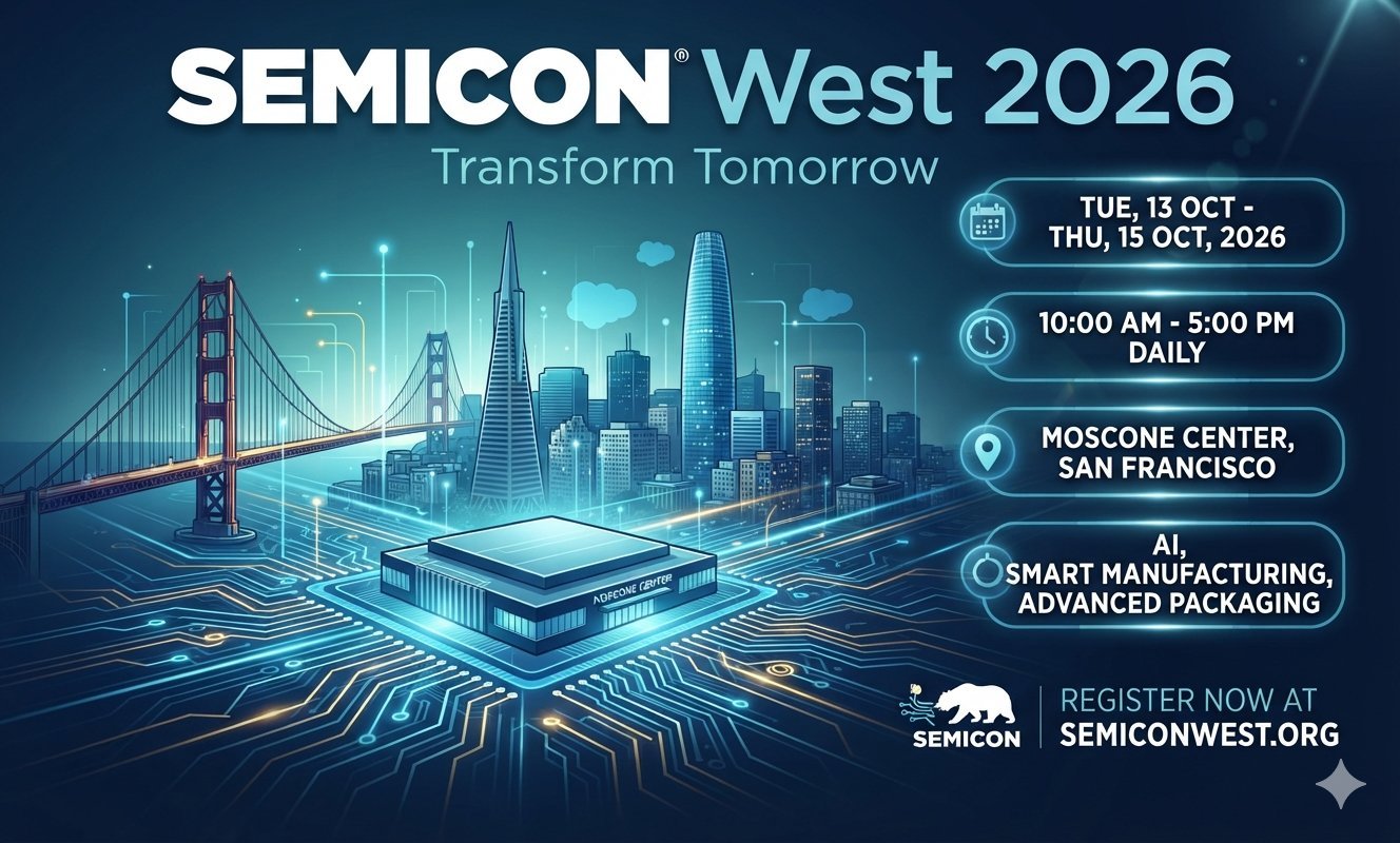
SEMICON West 2026 Moscone Convention Center
Trade Shows
Silicon Wafer Fab Equipment & Photolithography
Advanced Chip Packaging, Heterogeneous Integration & Test
Fab Automation, AI & Smart Manufacturing
Electronic Design Automation (EDA) & Sustainable Materials
THE WORLD’S PREMIER B2B EXPOSITION FOR SEMICONDUCTOR MANUFACTURING, MICROELECTRONICS & ADVANCED PACKAGING ARRIVES IN SAN FRANCISCO!
Organized by SEMI Global, the flagship autumn 2026 edition of SEMICON West brings together over 18,000+ C-suite executives, semiconductor foundry leaders, chip design engineers, materials scientists, and microelectronics equipment manufacturers from across North America, Europe, and Asia!
Hosted inside Moscone North & South Halls at the Moscone Center in San Francisco, California, United States, this high-impact 3-day global technology summit serves as the semiconductor ecosystem’s central design, wafer fabrication, and supply chain procurement floor—connecting photolithography tools, advanced 3D chip packaging, silicon wafer materials, quantum computing hardware, and AI-driven fab automation directly with global chipmakers and system integrators!
📅 Dates: Tuesday, October 13 – Thursday, October 15, 2026
⏰ Hours:
• Tuesday, Oct 13: Keynote & Exhibit Floor: 9:00 AM – 6:00 PM
• Wednesday, Oct 14: Keynote & Exhibit Floor: 9:00 AM – 6:00 PM
• Thursday, Oct 15: Keynote & Exhibit Floor: 9:00 AM – 4:00 PM
📍 Venue: Moscone Center (Moscone North & South Halls), 747 Howard St, San Francisco, CA 94103 (Silicon Valley Hub), United States
🎯 Target Audience: Semiconductor C-Suite Executives, Wafer Fab Operations Directors, Chip Design Engineers, Process Engineers, Packaging Specialists, R&D Scientists, Supply Chain Analysts, and Tech Investors.
✨ Key Exhibition Sectors & Microelectronics Technology Tracks:
🔬 Silicon Wafer Fab Equipment & Photolithography: Extreme ultraviolet (EUV) lithography systems, chemical vapor deposition (CVD), plasma etching tools, and automated wafer handling robotics.
📦 Advanced Chip Packaging, Heterogeneous Integration & Test: 2.5D/3D IC packaging architectures, substrate materials, wafer-level testing hardware, thermal management, and inspection systems.
🤖 Fab Automation, AI & Smart Manufacturing: AI-driven predictive maintenance software, digital twin fab simulation, IoT cleanroom monitoring, and supply chain optimization tech.
⚡ Electronic Design Automation (EDA) & Sustainable Materials: Chiplet design tools, silicon carbide (SiC) / gallium nitride (GaN) power semiconductors, ultra-pure gases, and green chemistry solutions.
🤝 Visionary Keynote Panels, Executive Business Matching & Global Networking: Access critical technical insights from 200+ industry thought leaders, evaluate live equipment demonstrations from 700+ global exhibitors, explore specialized pavilions (WFD, Smart Mobility, Smart MedTech), and network during executive networking receptions!
Power the future of global microelectronics live, source next-generation chip technology, and connect with Silicon Valley innovators in San Francisco!
#SEMICONWest #SEMICONWest2026 #SEMIGlobal #MosconeCenter #SanFrancisco #SiliconValley #Semiconductors #Microelectronics #ChipDesign #AdvancedPackaging #WaferFab #TechInnovation #B2BIndustrialExpo